The field of optoelectronics has seen significant advancements with the utilization of two-dimensional (2D) superconducting materials. These materials hold great promise for the development of miniaturized optoelectronic devices that can perform efficiently while consuming less energy. However, a key challenge in creating smaller devices is the need for a higher gate capacitance to store more electrical charge in proportion to the voltage applied. One approach to address this challenge is the use of insulating materials with a high dielectric constant (κ), such as hafnium oxide (HfO2). While this solution is advantageous, integrating these materials with 2D semiconductors has proven to be difficult.
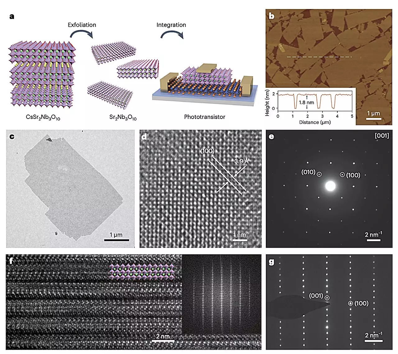
Recently, researchers at Fudan University have made a significant breakthrough by developing a 2D perovskite oxide with a high dielectric constant that can be integrated with various 2D channel materials. The paper detailing this research, published in Nature Electronics, highlights the potential of this new material in revolutionizing the down-scaling of optoelectronics. The 2D perovskite oxide, known as Sr2Nb3O10, was synthesized using a top-down preparation strategy and boasts a high dielectric constant (κ) of 24.6 along with a moderate bandgap.
The advantageous characteristics of Sr2Nb3O10 make it an ideal candidate for a photoactive high-κ dielectric in phototransistors based on various 2D semiconducting materials like graphene, molybdenum disulfide, tungsten disulfide, and tungsten diselenide. The researchers conducted experiments to evaluate the performance of transistors integrating Sr2Nb3O10 with different channel materials. The results showed promising outcomes, with molybdenum disulfide transistors exhibiting a high on/off ratio and tungsten disulfide phototransistors demonstrating excellent UV-visible dual-band photodetection capabilities.
The successful integration of Sr2Nb3O10 with various channel materials opens up new possibilities for developing smaller, better performing, and energy-efficient electronics and optoelectronics. The establishment of a well-defined interface between the semiconductor and dielectric, coupled with the high dielectric constant of Sr2Nb3O10, enables efficient gate control of channel materials. This breakthrough could pave the way for the synthesis of additional 2D perovskite oxides that can be seamlessly integrated with existing semiconductors, further advancing the field of optoelectronics.
The research conducted by Siyuan Li, Xinya Liu, and their collaborators sheds light on the immense potential of 2D perovskite oxides in revolutionizing optoelectronic device design and performance. With continued advancements in this area, we can expect to see even more innovative and efficient optoelectronic technologies in the near future.
Leave a Reply