The field of photonic integrated circuits is continually evolving, with a focus on the miniaturization and integration of photonic elements in chips. Unlike traditional electronic circuits that rely on electrons, photonic chips utilize photons for a range of calculations. Silicon-based photonics, a developing field with applications in data centers, artificial intelligence, and quantum computing, offers significant improvements in performance and cost-effectiveness. Although the lithography production process enables precise device production, accurately mapping the optic characteristics of these chips remains a challenge. This limitation inhibits the modeling of fabrication flaws and inaccuracies due to the chips’ small dimensions.
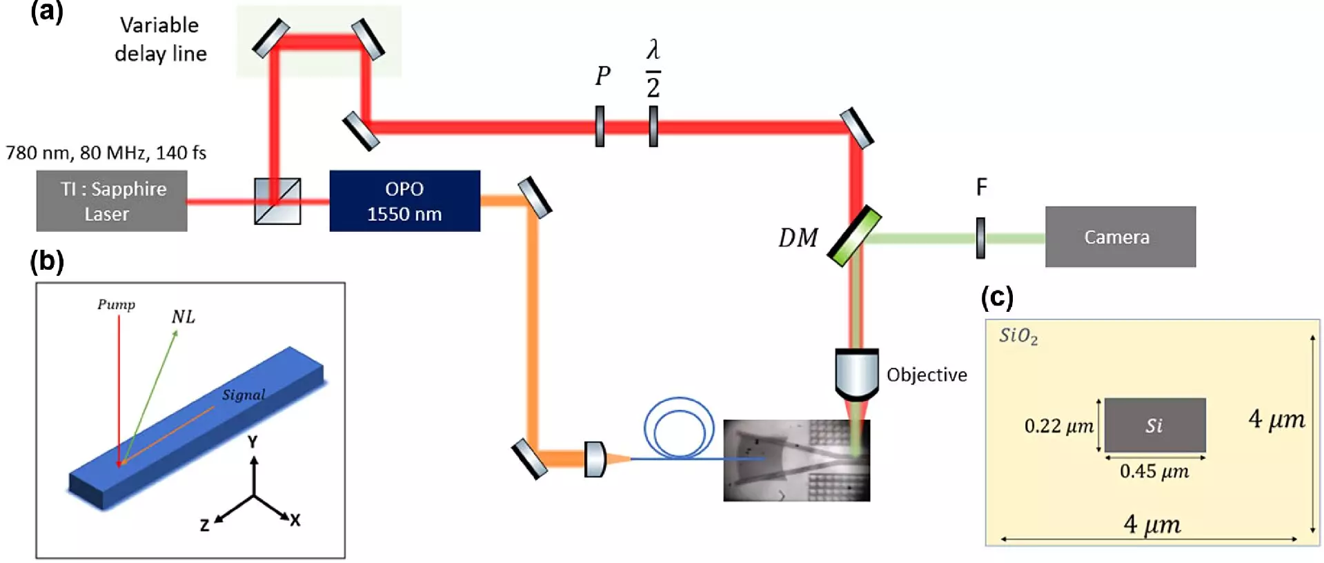
A recent article published in the journal Optica by researchers from Technion’s Andrew and Erna Viterbi Faculty of Electrical and Computer Engineering introduces a groundbreaking solution to this challenge. Led by Professor Guy Bartal and doctoral student Matan Iluz, the team developed a method for advanced light imaging in photonic circuits on chips. Collaborating with Professor Amir Rosenthal’s research group, the researchers harnessed the optical characteristics of silicon to map the movement of light within the chip without invasive actions that perturb or alter the chip’s structure.
The process involves mapping the electric field of the light waves and identifying the elements that affect its movement, such as waveguides and beam splitters. By leveraging the properties of silicon, the researchers were able to capture real-time images and videos of the light inside the photonic chip. Unlike previous methods that often required damaging the chip or losing critical data, this new process allows for non-invasive mapping of the light’s propagation.
The researchers’ innovative approach holds immense potential for improving the design, production, and optimization processes of photonic chips across diverse fields. The telecommunications industry can benefit from more accurate mapping, enabling the development of faster and more efficient data transfer. High-performance computing and machine learning can leverage this advancement to enhance computational speed and power. Furthermore, fields like medical imaging and sensing can utilize this technology to improve diagnostic capabilities and measurement accuracy. Finally, the field of quantum computing, which relies on the delicate manipulation of photons, can greatly benefit from the precise mapping of light propagation.
The research conducted by Technion’s researchers presents a significant breakthrough in the field of photonic integrated circuits. By harnessing the optical properties of silicon, they have developed an advanced light imaging method that enables the accurate mapping of light propagation within photonic chips. This non-invasive approach has the potential to revolutionize various industries, including telecommunications, high-performance computing, machine learning, medical imaging, sensing, and quantum computing. As this technology continues to evolve, it holds the promise of unlocking new possibilities in the realm of photonics and amplifying the capabilities of photonic integrated circuits.
Leave a Reply