Researchers in Singapore have created a sub-wavelength LED, which is smaller than the wavelength of light, that can be used to convert mobile phone cameras into high-resolution microscopes. Using modifications to the silicon chip and software, existing camera devices in everyday items such as mobile phones can be converted into microscopes. The revolutionary neural networking algorithm developed by the research team can reconstruct microscopic objects such as cells and bacteria without the need for bulky conventional microscopes or additional optics. This breakthrough can significantly advance diagnostics for indoor farmers and sustainable agriculture. The technology paves the way for a powerful on-chip emitter that is smaller than a micrometer and could transform the field of photonics.
Novel Deep Neural Network Architecture
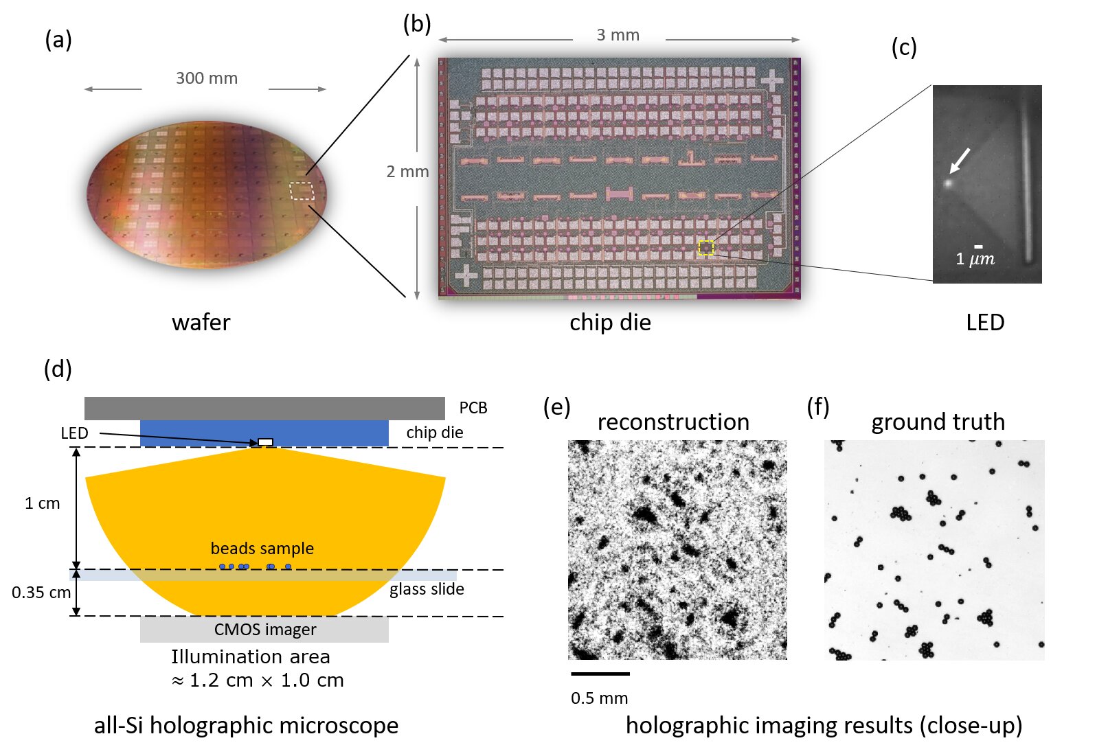
The researchers also unveiled a novel deep neural network architecture capable of reconstructing images from a holographic microscope. The neural network incorporates total variation regularization for increased contrast and takes into account the wide spectral bandwidth of the source. Unlike traditional methods of computational reconstruction that require training data, this neural network eliminates the need for training by embedding a physics model within the algorithm. The untrained neural network allows researchers to use novel light sources without prior knowledge of the source spectrum or beam profile. The researchers envision that this synergetic combination of CMOS micro-LEDs and the neural network can be used in other computational imaging applications, such as a compact microscope for live-cell tracking or spectroscopic imaging of biological tissues such as living plants.
The researchers developed the smallest reported Si emitter with a light intensity comparable to that of state-of-the-art Si emitters with much larger emission areas. The unique LED is a CMOS-integrated sub-wavelength scale LED exhibiting high spatial intensity and possessing the smallest emission area among all known Si emitters in scientific literature. The LED can be combined into an array for higher levels of illumination for larger-scale applications without increasing the system’s complexity, cost, or form factor. Control electronics and even the imager could also be integrated into the same chip, creating an all-in-one micro-LED that could be transformative for the field. The LED has a wide range of possible applications, including bio-imaging and bio-sensing applications and on-chip communication, NIR proximity sensing, and on-wafer testing of photonics.
Leave a Reply