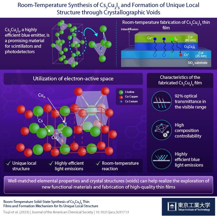
The use of high-quality materials, such as metal halide phosphors, is essential in advanced electronic devices to efficiently convert light into measurable signals. One of the most promising materials is cesium copper iodide (Cs3Cu2I5: CCI), a toxic element-free copper-based iodide that is an efficient blue light-emitting material that can convert almost all the absorbed energy into detectable light. However, thin films of CCI do not meet the necessary quality standards, hampering their performance in advanced stacking applications.
The Study
Researchers at the Tokyo Institute of Technology have proposed a new method for creating high-quality thin films of Cs3Cu2I5. The team discovered that cesium iodide (CsI) and copper iodide (CuI) powders can react even at room temperature to form Cs3Cu2I5. They then deposited thin films of CuI and CsI onto a silica substrate by evaporating them in a vacuum chamber. The two films were allowed to react at room temperature to form transparent and highly smooth films with a high optical transmittance of 92%. The order in which the layers were deposited affected the formed crystalline phases. The deposition of CsI over CuI resulted in the formation of a blue light-emitting thin film of Cs3Cu2I5, which is the equilibrium phase under this thickness ratio condition.
The researchers found that the interdiffusion process leads to the formation of distinct local structures containing point defects that decay through nonradiative channels upon photoexcitation, resulting in highly efficient emissions. Using this approach, the researchers were able to fabricate patterned thin films by selectively depositing a CsI layer through a shadow mask. This allowed them to control the deposition of CsI and pattern only the desired area of the substrate. By carefully adjusting the thickness of the CuI and CsI layers, they were able to successfully fabricate a film with a central blue light-emitting Cs3Cu2I5 region bordered by a yellow light-emitting CsCu2I3 region.
The Implications
The researchers believe that their findings could lead to the development of high-quality thin film devices with ideal optical properties for advanced stacking applications. The ability to create patterned thin films could also open up new possibilities for future applications. The researchers demonstrated that the same thin films can be obtained by using solution-processed CuI and patterned CsI thin films. The photoluminescent properties of Cs3Cu2I5 originate from the unique local structure around the luminescent center, the asymmetric [Cu2I5]3−polyhedron iodocuprate anion, consisting of the edge-shared CuI3 triangle and the CuI4 tetrahedron dimer that is isolated by Cs+ ions.
The researchers argue that the interdiffusion process leads to the formation of distinct local structures containing point defects that decay through nonradiative channels upon photoexcitation, resulting in highly efficient emissions. “Our study explains the mechanism underlying the formation of the rare local structures in Cs3Cu2I5 and its association with photoluminescence in these materials. These results can ultimately pave the way for the development of high-quality thin film devices with ideal optical properties for advanced stacking applications,” concludes Prof. Hosono.
Leave a Reply