In a recent breakthrough, researchers at the ARC Center of Excellence for Transformative Meta-Optical Systems (TMOS) and RMIT University have unveiled a cutting-edge 2D quantum sensing chip using hexagonal boron nitride (hBN). This innovative chip has the ability to simultaneously detect temperature anomalies and magnetic fields in any direction, marking a significant advancement in the field of quantum technology.
Traditionally, quantum sensing chips have been constructed from diamond due to its robust nature. However, diamond-based sensors are limited in their capacity to detect magnetic fields only when aligned in the direction of the field. This limitation results in large blind spots and the necessity for multiple sensors at varying alignments, making the operation more complex and less versatile for different applications.
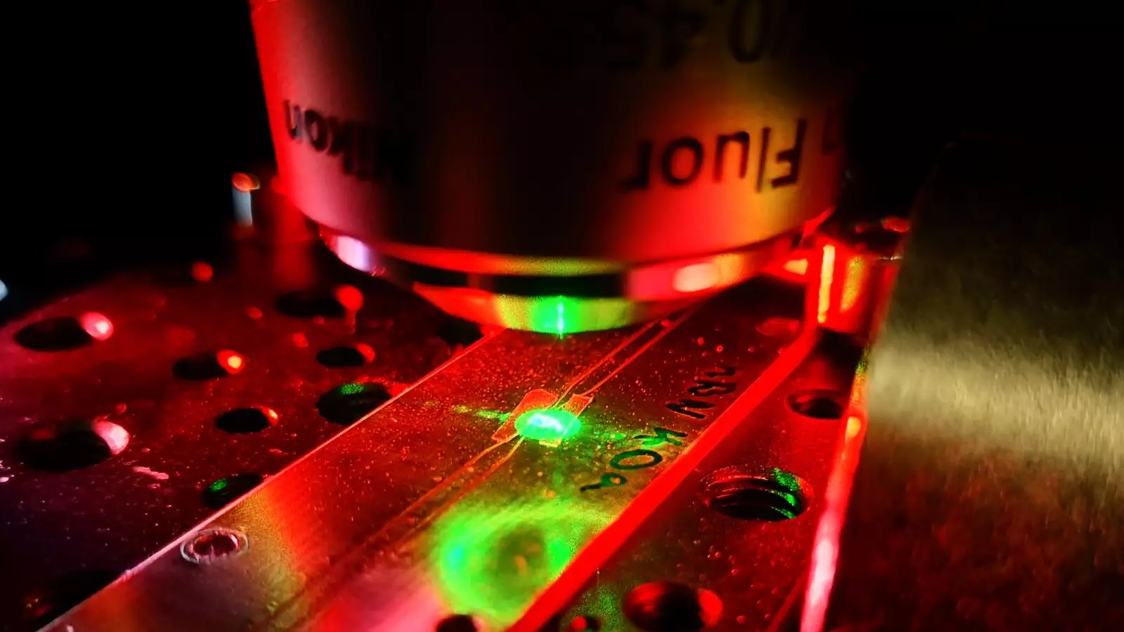
By utilizing hBN crystals, the research team led by TMOS Associate Investigator Jean-Philippe Tetienne and Chief Investigator Igor Aharonovich has revolutionized quantum sensing technology. These atomically thin hBN crystals offer flexibility, allowing the sensing chips to conform to the shape of the sample being studied. Unlike diamond sensors, hBN sensors can get much closer to samples, enabling more precise measurements.
The Discovery of a Carbon-Based Defect
One of the key discoveries made by the research team was a carbon-based defect in hBN that had not been previously utilized for magnetic imaging. Through a Rabi measurement experiment, the team identified this defect as a spin half system, enabling the sensor to detect magnetic fields in any direction. This breakthrough has opened up new possibilities for quantum sensing applications.
The development of the hBN quantum sensing chip has vast implications for various fields. Co-first author Priya Singh highlights the potential for utilizing hBN sensors in biological systems, where their directional independence can be advantageous. Moreover, TMOS Chief Investigator Igor Aharonovich emphasizes the advantages of hBN over diamond, citing its thin form factor and room temperature operation.
Looking ahead, TMOS Associate Investigator Jean-Philippe Tetienne underscores the importance of identifying atomic defects in hBN to further enhance the performance of sensor devices. By delving into the properties of these defects, the research team aims to optimize the quantum sensing capabilities of hBN and explore new opportunities in the realm of quantum materials.
The development of the 2D quantum sensing chip utilizing hBN crystals represents a significant step forward in quantum technology. The ability to detect temperature anomalies and magnetic fields in any direction opens up a wide range of applications in various fields, from biological systems to geological exploration. With ongoing research and advancements, the potential for quantum sensing technology using hBN is truly groundbreaking.
Leave a Reply