Semiconducting materials that are two-dimensional (2D) in nature have been the subject of much research due to their unique optoelectronic properties. These materials hold great potential for the development of ultra-thin and tunable electronic components. However, one of the challenges faced by researchers has been effectively interfacing these materials with gate dielectrics without encountering interfacial traps that degrade transistor performance. Recently, researchers from King Abdullah University of Science and Technology (KAUST), Soochow University, and other institutions worldwide introduced a novel approach that could revolutionize the fabrication of high-performance transistors based on 2D semiconductors.
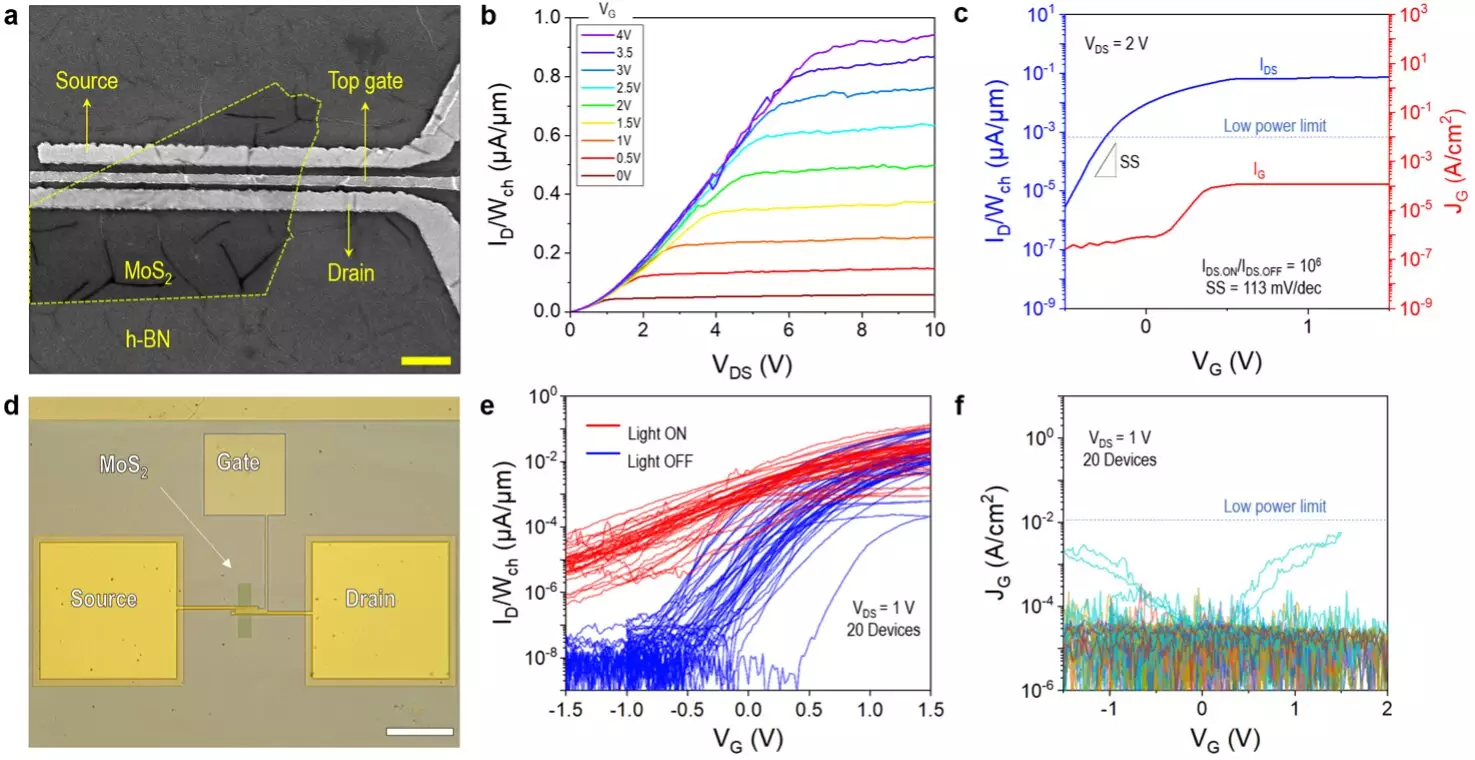
The proposed design outlined in a paper published in Nature Electronics involves the use of hexagonal boron nitride (h-BN) dielectrics and metal gate electrodes with a high cohesive energy. Initial experiments involving platinum (Pt) as an anode revealed that the h-BN stack is less likely to trigger dielectric breakdown. This crucial finding led the research team to further investigate the potential of h-BN gate dielectrics in 2D transistors. The use of chemical vapor deposited h-BN dielectrics in over 1,000 fabricated devices yielded significantly lower leakage current and a high dielectric strength when paired with high cohesive energy metals like Pt and tungsten (W).
To fabricate transistors with a vertical Pt/h-BN/MoS2 structure, the researchers employed a meticulous fabrication process. Starting with a clean SiO2/Si substrate, source and drain electrodes were patterned using electron beam lithography and deposited. The MoS2 channel was created by transferring exfoliated MoS2 onto the electrodes, followed by the placement of CVD h-BN film via wet transfer. The final step involved patterning the Pt gate electrode using electron beam lithography and depositing it using e-beam evaporation. This process resulted in a clean van der Waals interface between MoS2 and h-BN, enhancing the transistor’s reliability and performance.
Contrary to common belief that CVD h-BN is a poor gate dielectric, the research team’s findings highlight the effectiveness of this material when paired with the right metal electrodes. The clean van der Waals interface formed between MoS2 and h-BN demonstrates the potential for reliability improvement. By utilizing high cohesive energy metals such as Pt and W, CVD h-BN proves to be a viable gate dielectric choice for 2D transistors. The reduction in leakage current and improved dielectric strength pave the way for the development of reliable solid-state microelectronic circuits and devices based on 2D materials.
The promising results obtained by Shen and her colleagues indicate a bright future for 2D semiconductor-based transistors. The significant reduction in current leakage achieved through the use of Pt and W-based gate electrodes suggests the potential for highly performing 2D semiconductor devices. This research opens up possibilities for the exploration of new approaches and materials by other research groups, ultimately contributing to the advancement of 2D semiconductor technology. As the research team plans to delve into the development of ultra-small, fully 2D transistors, the future looks bright for the integration of 2D semiconductors in electronic components to extend the limits of Moore’s Law.
Leave a Reply