The concept of manipulating materials to exhibit unique properties based on their thickness is truly remarkable. When materials are reduced to just one or two layers of molecules, they can undergo a transformative process. This phenomenon is at the core of the research conducted by physicist Prof. Ursula Wurstbauer and her team at the University of Münster. The team’s focus is on exploring how two-dimensional crystals can be engineered to act as insulators, electrical conductors, superconductors, or ferromagnets, among other functionalities.
A groundbreaking aspect of the team’s research is the generation and quantification of collective excitations of charge carriers within different energy landscapes. By leveraging the interactions between electrons and the energy landscape of crystals, the researchers have shed light on the electronic behaviors of crystal structures and uncovered methods to influence them. The findings of their study, recently published in Physical Review Letters, mark a significant advancement in our understanding of two-dimensional materials.
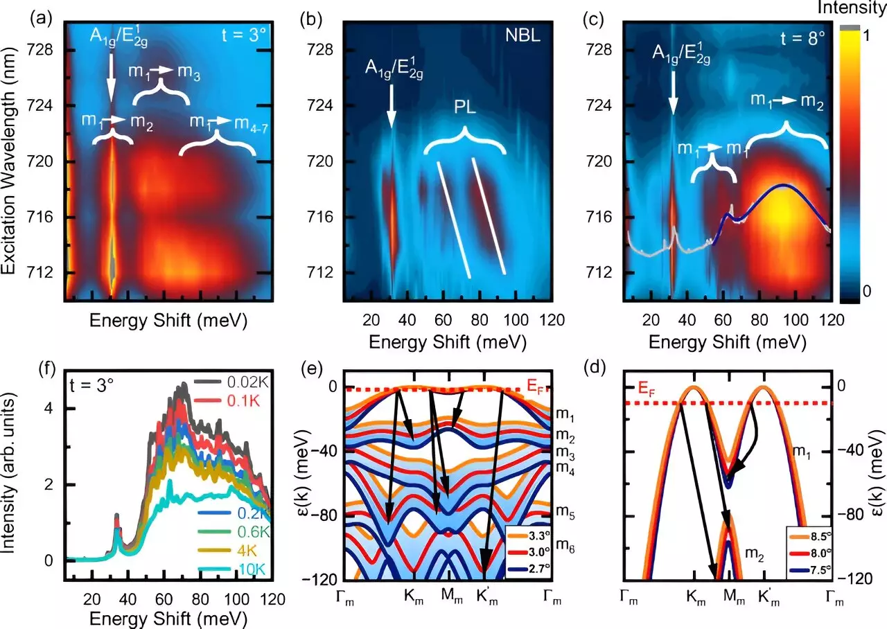
To achieve distinct properties in two-dimensional crystals, the researchers employed a method of stacking two layers of the material and slightly twisting them relative to each other. This twisting action generates moiré patterns, akin to overlaid layers of thin fabric. These patterns define the energy landscape of the crystals, causing electrons to move at a slower pace and interact more intensely with each other. Consequently, these altered conditions can lead to strongly correlated behaviors among electrons, where they exhibit unique dance-like movements compared to their traditional behavior.
Applications Beyond Basic Research
While the electronic characteristics of these material systems are captivating from a fundamental research perspective, Prof. Wurstbauer envisions broader applications in quantum technology and neuromorphic components. The unique properties exhibited by these engineered two-dimensional crystals could pave the way for innovative technological advancements, offering new possibilities for the development of advanced circuits and devices.
The research conducted by Prof. Wurstbauer’s team represents a collaborative effort involving experts from various institutions, including the University of Hamburg, RWTH Aachen University, and the Max Planck Institute for the Structure and Dynamics of Matter in Hamburg. By combining experimental work with theoretical analyses, the team was able to explore different two-dimensional crystals such as graphene, molybdenum diselenide, and tungsten diselenide. Through optical spectroscopy methods at cryogenic temperatures, known as resonant inelastic light scattering spectroscopy, the researchers gained critical insights into the unique characteristics of these materials.
The study of two-dimensional crystals and their ability to manifest distinct properties through controlled manipulations offers a glimpse into the fascinating world of materials science. As researchers continue to delve deeper into the complexities of these materials, the potential for groundbreaking discoveries and technological innovations looms on the horizon.
Leave a Reply