In a pioneering achievement, researchers from UC Santa Barbara have unveiled the first live visualization, or “movie,” of electric charges navigating the interface between two distinct semiconductor materials. This extraordinary advancement, facilitated by the scanning ultrafast electron microscopy (SUEM) techniques developed in the lab of Bolin Liao, represents a significant milestone in our understanding of charge carrier dynamics. Liao, an associate professor of mechanical engineering, emphasized the importance of this breakthrough, noting the limitations of traditional semiconductor theory which often relies on indirect measurements. This experimental visualization allows semiconductor scientists to validate and refine established theoretical frameworks.
The phenomenon of charge movement in semiconductor materials, particularly during events triggered by sunlight in solar cells, has long been a subject of academic inquiry. When light hits these materials, it energizes electrons, prompting them to move and generating a flow of electric current. However, the majority of these photocarriers dissipate their energy rapidly, within picoseconds, leading to a loss of potential energy that could otherwise enhance the efficiency of solar cells and other devices. Understanding the behavior of hot carriers—the excited electrons before they lose energy—is crucial, as their dynamics can significantly influence device performance.
The rapid energy loss in photocarriers poses challenges, as the resulting heat can adversely affect the operation of semiconductor devices. Therefore, gaining insights into how these hot carriers behave as they traverse different materials—most critically, at the junction of two disparate semiconductors commonly known as a heterojunction—becomes essential. Heterojunctions play vital roles in diverse applications, such as lasers, photovoltaic cells, sensors, and photocatalysis, making it imperative to unravel the intricacies of charge carrier movement across these interfaces.
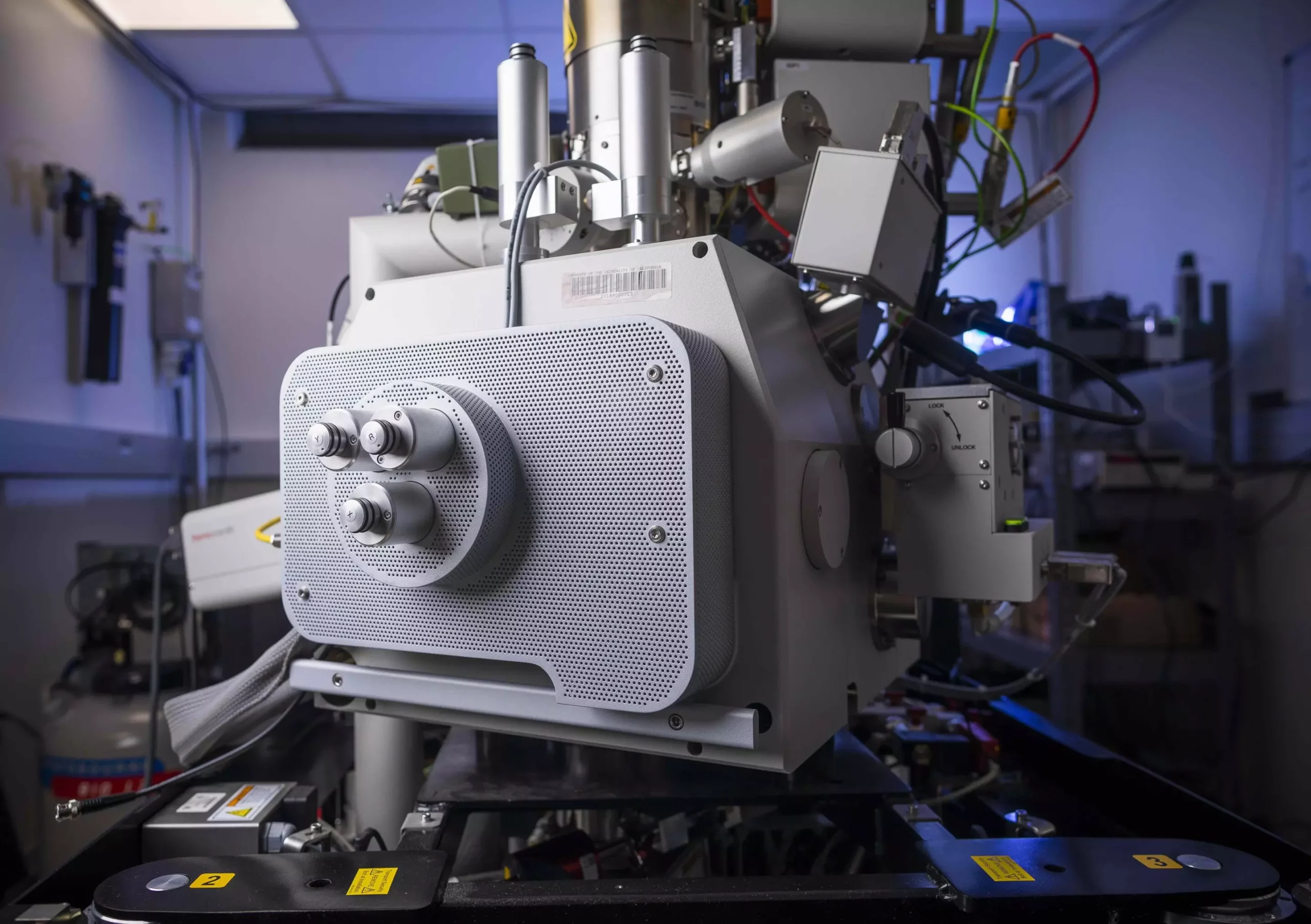
In their groundbreaking research, Liao and his team utilized SUEM to focus on a heterojunction formed by silicon and germanium, two of the most prevalent semiconductor materials. This choice opens avenues for innovation in areas like telecommunications and photovoltaic applications. By employing ultrafast laser pulses as a picosecond-scale shutter while firing an electron beam, the researchers were able to capture time-resolved images of the movement of hot photocarriers as they were excited by an optical pump beam.
“What we are observing occurs within a very short timeframe; between picoseconds and nanoseconds,” Liao remarked. The implications of this ability to visualize charge movement are profound, offering insights into how excitations transfer and flow across semiconductor interfaces. Such visualization is not only a scientific achievement but also serves as a bridge to enhance practical applications of semiconductor technology.
The findings reveal fascinating aspects of charge dynamics. When photocarriers are excited within homogeneous regions of silicon or germanium, they exhibit rapid movement due to their high-energy states. However, at the heterojunction interface, a proportion of these carriers become trapped by the junction potential, resulting in a decrease in their mobility. This phenomenon signifies potential performance hindrances in devices designed to separate and collect these hot charges. While theories in semiconductor physics had anticipated the charge trapping effect, witnessing it through direct experimental observation was a surprising breakthrough for Liao and his team.
“We did not expect to capture this effect so vividly,” he stated, underscoring the potential ramifications for semiconductor device design. The insights gained from this study not only illuminate fundamental aspects of semiconductor behavior but also provide critical data that engineers and designers can use to optimize device performance.
This groundbreaking research at UC Santa Barbara completes a significant chapter in semiconductor studies that traces back to the visionary work of late professor Herb Kroemer. In 1957, Kroemer introduced the concept of heterostructures in semiconductors, famously asserting that “the interface is the device.” This foundational idea has been instrumental in shaping modern technologies, including microchips and computers.
The ability to visualize hot photocarrier activity at heterojunctions reinforces UCSB’s reputation in semiconductor research and opens new avenues for exploration. As researchers continue to investigate the dynamics of charge carriers and their implications for device efficiency and performance, we stand at the threshold of a new era in semiconductor technology—one that promises enhanced energy efficiency and transformative advancements across various electronic applications. The potential to bridge theoretical predictions with direct observation heralds a new age for innovation in semiconductor devices.
Leave a Reply