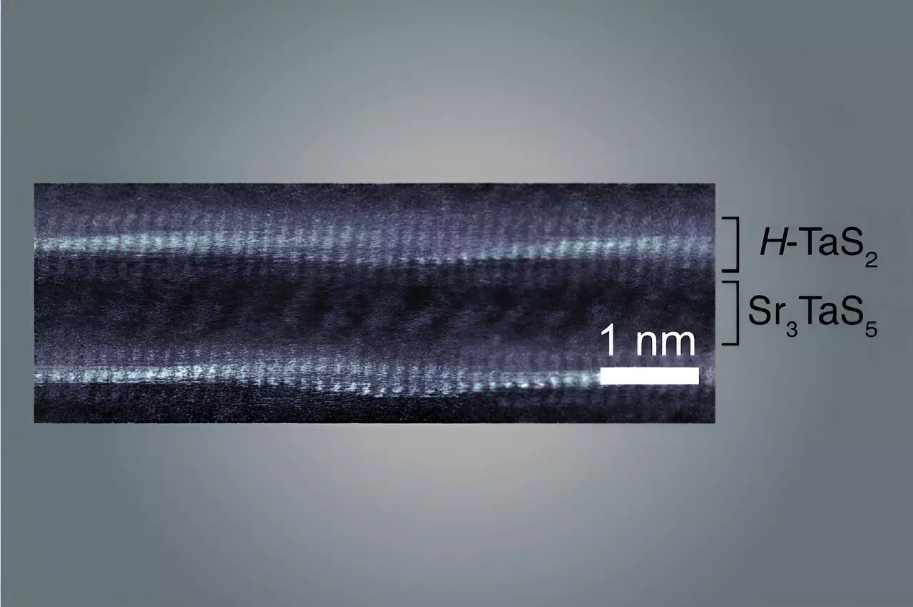
In a groundbreaking development, researchers from MIT have unveiled a new material characterized by its unique superconducting and metallic traits, made possible through the creation of wavy atomic layers that measure only billionths of a meter in thickness. Unlike conventional materials, which often exist in less manipulable formats, this newly developed material is structured to form macroscopic samples. This substantial size aids scientists in investigating the quantum behaviors that underline its extraordinary properties. Published in the prestigious journal *Nature*, this research signifies an essential leap in material science, as it illustrates a rational design approach that meticulously curates the composition and structure of the material, ultimately expanding the palette of materials available for exploration and application.
What distinguishes this newly synthesized material from others is its intricate layered structure, akin to a meticulously crafted layer cake. At its core, the material comprises alternating layers of tantalum and sulfur juxtaposed against a layer of strontium, tantalum, and sulfur. These layers duplicate themselves thousands of times, resulting in a crystal formation that is uniform and stabilized across its expanse. As explained by Joseph Checkelsky, the project’s senior investigator and an associate professor of physics at MIT, the uniformity of this wave-like atomic pattern befuddles traditional crystal classifications, urging researchers to explore the emergent physical properties that could stem from this complexity.
The scientific community has increasingly focused on two-dimensional materials that consist of one or just a few atomic layers. These materials are recognized for their modifiable properties that can yield unprecedented effects by manipulating their configurations. One exciting technique involves twisting the atomic layers to create a moiré superlattice, which leads to phenomena such as superconductivity and unconventional magnetism. Despite its promise, the development and examination of moiré materials pose significant challenges. Traditional assembly methods are not only labor-intensive but also hindered by the minute dimensions of the materials involved. Researchers like Checkelsky have thus turned their attention to alternative methods that simplify these processes without compromising the material’s integrity.
The method utilized by Checkelsky’s team marks a radical innovation in material synthesis. Instead of laboriously assembling layers by hand, they have streamlined the process to involve mixing powdered materials and subjecting these mixtures to high temperatures in a furnace. This method encourages seamless chemical reactions that allow for the automatic formation of large crystals, defined by their atomic-scale interactions. This pivotal transition from manual to automated assembly not only enhances efficiency but also promises a new avenue for the systematic exploration of materials that express unique behaviors due to tailored atomic arrangements.
One notable aspect of this new material is how its wavy structure results from the intrinsic mismatch between the crystal lattices of its constituent layers. Such disparities cause one layer to undergo a buckling transformation to align properly with those below it, thereby creating wave formations that influence the overall behavioral dynamics of the material. The analogy of placing a sheet of legal paper over regular printer paper aptly illustrates this process; the legal paper must bend at specific points to fit correctly above, generating the waves that are crucial to the material’s properties.
This wave-like structure has profound implications for superconductivity. At a specific threshold of temperature, the material facilitates a state where electrons traverse through it without resistance. The alignment modulated by the wavy structure means that superconductivity can exhibit variability throughout the material, presenting zones of enhanced conductivity interspersed with areas of diminished flow. Moreover, the wavy architecture directs electron movement, making their flow more efficient in specific directions. This directionality not only enhances electron mobility but also allows for the fine-tuning of electrical properties that could support advanced applications in various tech fields.
As researchers like Aravind Devarakonda delve deeper into the behavior of this newly uncovered material, they recognize its potential as a foundational element for an entirely new class of materials. The exploration of the structural modulations and their interactive behaviors could revolutionize fields ranging from quantum computing to energy storage solutions. The results of this research mark just the beginning; as Checkelsky puts it succinctly, they have “planted the flag,” inviting further exploration and the possibility of uncovering even more materials with outstanding properties. The ever-expanding frontier of material science now holds an exciting promise for the future of technology, with surprising opportunities lying in wait for innovative applications.


Leave a Reply