As the integration of artificial intelligence (AI) into various sectors escalates, the demand for robust data processing and storage solutions has become more pronounced. AI relies heavily on data analysis, and as datasets grow in size and complexity, traditional memory technologies struggle to keep pace. The need for higher memory bandwidth and faster data transfer rates is critical, not just for enhanced performance, but also for energy efficiency. High-bandwidth memory technologies are emerging as potential frontrunners in addressing these demands, yet they come with their own challenges.
Currently, flash memory dominates the landscape of non-volatile storage solutions, allowing data retention even when devices are powered down. However, conventional flash memory technologies often fall short of the speed requirements needed for advanced applications such as AI, leading to a concerted effort from researchers to develop alternatives that maximize both efficiency and speed.
Recent advances in the field of two-dimensional (2D) materials present exciting opportunities for the creation of next-generation flash memory devices. Engineers have explored the facilitation of ultrafast data processing through the use of 2D materials, which have unique electrical properties that can be harnessed for superior performance. Research efforts at Fudan University, for example, have demonstrated that ultrafast flash memory devices can be constructed from exfoliated 2D materials. However, while these long-channel devices exhibited impressive speeds, their scalable integration for mass production remained a formidable obstacle.
Addressing this issue, recent studies have proposed innovative integration techniques that promise to enhance the commercialization of ultrafast flash memory. By tackling the challenges of interface engineering, researchers not only aim to improve the performance of memory devices but also strive to develop methods that facilitate their deployment on a larger scale.
The researchers at Fudan University have outlined a groundbreaking approach for the scalable integration of 1,024 ultrafast 2D flash memories, achieving an impressive yield exceeding 98%. Their reported method combines various fabrication techniques, including lithography, e-beam evaporation, thermal atomic layer deposition, and novel polystyrene-assisted transfer processes. This multidisciplinary approach enables the creation of memory stacks with distinct tunneling barrier configurations, showcasing the versatility of the technology.
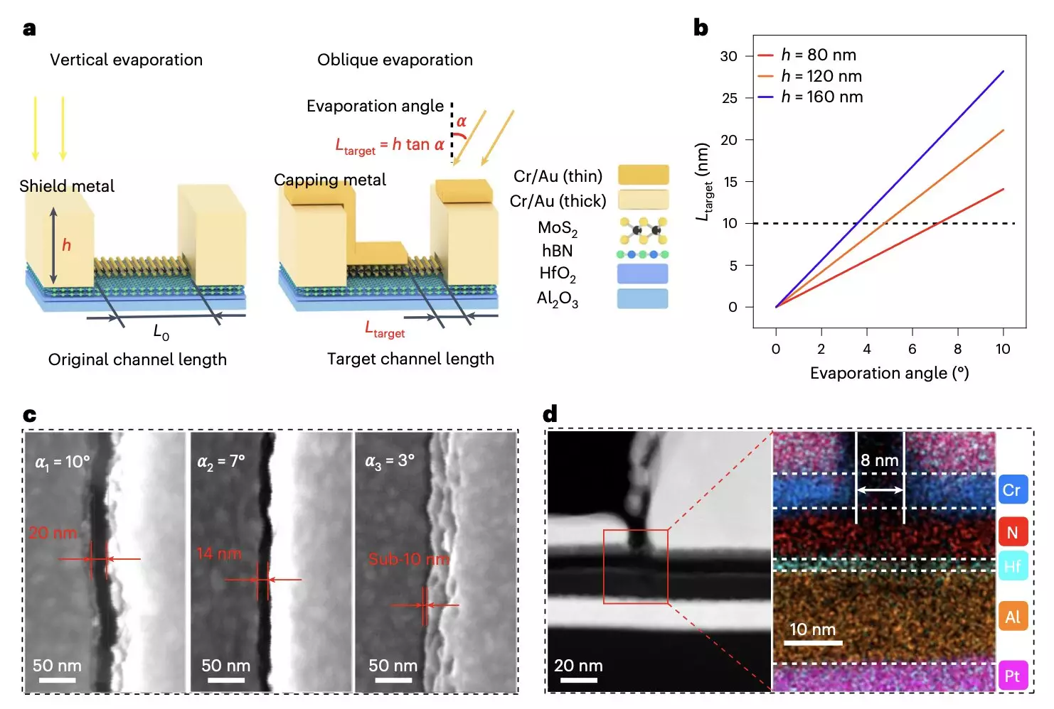
In their experiments, the team demonstrated the fabrication of memory devices capable of maintaining ultrafast performance even with channel lengths reduced to sub-10 nanometers—well below the limitations of traditional silicon flash technology. Each device exhibited remarkable data retention capabilities, boasting non-volatile information storage of up to four bits and durability extending far beyond 105 cycles. These advancements signal a significant leap forward for memory technology, potentially enabling smoother and faster AI applications.
The implications of these findings are profound. With the feasible integration of ultrafast 2D flash memory, a new frontier of storage solutions arises—one that can support the demanding computational requirements of AI and other high-performance applications. Researchers suggest that their processes may extend beyond a single material scope, paving the way for arrays that utilize various 2D materials and alternative memory stack configurations.
Future exploration into these ultrafast memory technologies and their scalability could significantly impact industries dependent on real-time data processing, including but not limited to AI, big data analytics, and cloud computing. As universities and technology companies pursue further experimental avenues, the potential for a robust, high-speed data storage ecosystem becomes increasingly tangible.
As the digital landscape continues to evolve, the need for more advanced memory solutions becomes indisputable. The research conducted by the team at Fudan University represents a significant milestone in the development of ultrafast 2D flash memory, fostering hope for enhanced data storage capabilities that align with the relentless pace of technological advancement. As further studies unfold, we may find ourselves on the cusp of a new era in data storage that not only meets the needs of current applications but also anticipates and prepares for the challenges posed by future innovations.
Leave a Reply