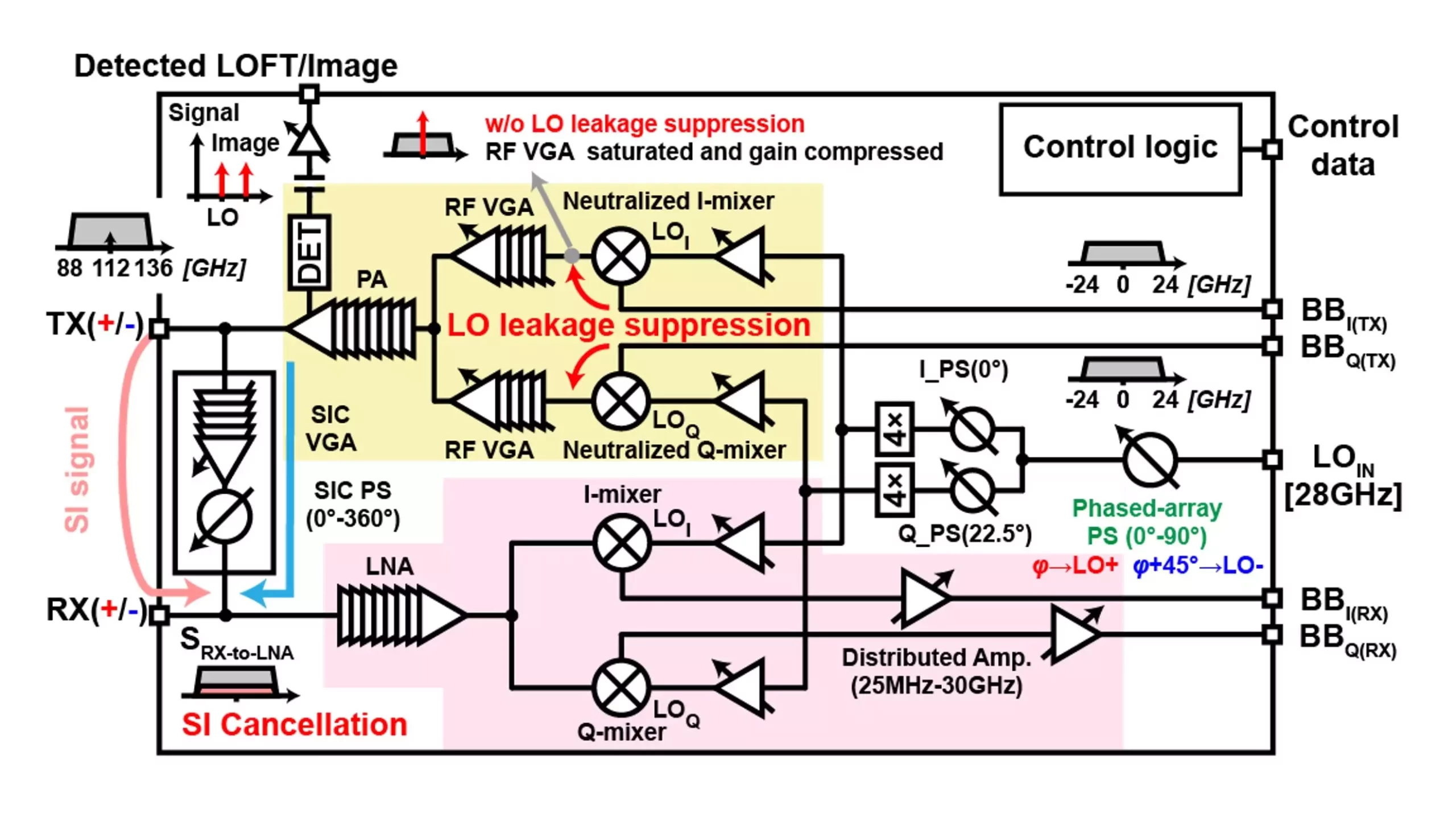
Scientists and engineers in the telecommunications industry are already working on the technologies that will be used for the sixth generation (6G) networks. Ideally, 6G should deliver data rates of over 100 gigabits per second (Gb/s) and support extremely low latencies for applications such as autonomous cars and virtual reality. The new transceiver design capable of both transmission and reception at frequencies over 100 GHz and at 112 Gb/s data rate could pave the way to 6G technologies.
The Full-Duplex Architecture
One way to meet the massive requirements for transmission and reception is to adopt a full-duplex (FD) architecture operating at sub-THz frequencies from 88 to 136 GHz. The main advantage of the FD architecture is that it enables a single system to both transmit and receive signals, effectively doubling the throughput. One way to implement this architecture is to make the transmission and reception modules share a single antenna. This helps reduce the size of the circuit and allows both parts to make full use of the available frequency spectrum.
However, single-antenna FD architectures suffer greatly from self-interference (SI), a phenomenon in which the transmitted signal leaks into the receiver side. Such systems must include circuits for SI cancelation that attempt to cancel the generated SI by injecting an equal signal with the opposite polarity. In the sub-THz band, implementing effective SI cancelation is much more challenging than in lower frequencies, which remains a hurdle to single-antenna FD designs.
The Novel FD Communication System
A team of researchers from Tokyo Institute of Technology (Tokyo Tech), Japan, have recently developed a novel FD communication system addressing the obstacles posed by SI. The research team of Professor Kenichi Okada presented their design at the 2023 Symposium on VLSI Technology and Circuits held June 11-16, Kyoto, Japan.
One of the main features of their system is the implementation of a dual-polarized patch antenna. It is driven by differential signals—a combination of positive and negative feeding ports for transmission and reception. By making the circuit paths of these ports highly symmetrical, the mismatch of the transmitted signal that leaks into the differential receiver’s ports is minimized, which helps keep SI low.
Another important aspect of the proposed design is the SI cancelation (SIC) circuit. For effectively canceling the generated SI, one needs to carefully modify the phase of the cancelation signal such that it is opposite to that of the leaked signal. This is usually done using variable capacitors called varactors. However, at the sub-THz range, conventional varactors have a limited phase range and poor resolution. To tackle this problem, the researchers developed a new varactor structure that achieved excellent linear resolution over the entire sub-THz band and over the full 360° range.
The Test Results
The team tested their design through a series of experiments, which yielded quite promising results. “In the over-the-air measurement, the proposed FD transceiver achieved 6 Gb/s. The SI suppression was improved by 20 decibels when the SI canceler was turned on,” says Prof. Okada.
The device, the world’s first FD phased-array transceiver to operate at over 100 GHz, also achieved a data rate of 112 Gb/s in HD mode. This is the fastest-to-date system among sub-THz phased-array transceivers. Together with a compact size and a wide range of operating frequencies, the proposed architecture represents a big step toward the telecommunications technology for 6G.
The new transceiver design developed by the researchers from Tokyo Tech is capable of both transmission and reception at frequencies over 100 GHz and at 112 Gb/s data rate. The proposed architecture reaches unprecedented data rates while maintaining a surprisingly compact size, representing a big step toward the telecommunications technology for 6G.


Leave a Reply