Organic semiconductors have come a long way since the 1980s when thin-film devices were first introduced. From OLED displays to programmable lighting and biosensors, these materials have found increasing applications in various technologies. The recent surge in wearable electronics has pushed the boundaries of device resolutions, particularly in near-eye displays like virtual and augmented reality devices.
A review published in the journal Wearable Electronics highlights the work done by scientists from Germany and China in developing a photolithography-compatible technology for ultra-high-resolution organic semiconductor devices. Traditionally, inorganic semiconductors like silicon have achieved incredibly small device dimensions using photolithographic technology. However, applying this to organic materials has proven challenging due to the degradation caused by UV light and solvents.
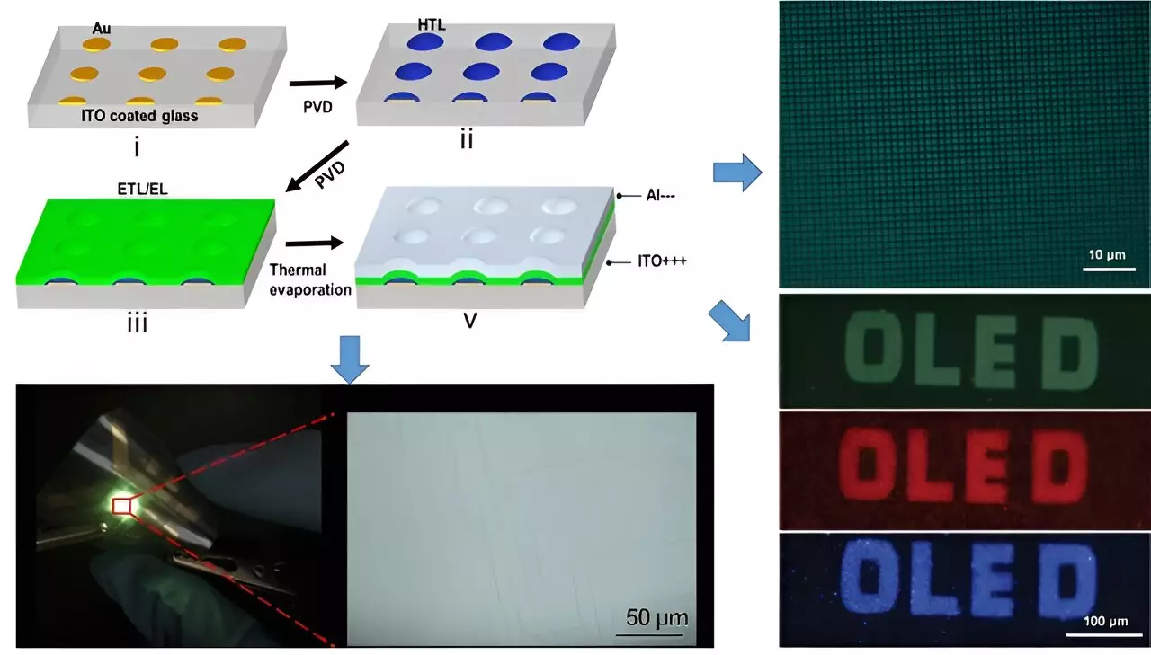
To overcome this hurdle, the researchers introduced a novel approach of “first surface patterning and then patterned growth.” This method involved patterning the substrate surface with lithography before introducing organic materials. Subsequently, organic semiconductor molecules were deposited, diffused on the surface, and selectively grown at specific areas, allowing for pattern formation and device fabrication on substrates.
The results of this approach were remarkable, with OLEDs reaching resolutions of over 20K pixels per inch, meeting the demands of next-generation displays. The lead investigator of the study, Lifeng Chi, emphasized that this method avoids damage to organic semiconductors during lithographic procedures, offering significant advantages in surface engineering and device resolution. The vision for future wearable electronics includes the seamless integration of multifunctional systems on a chip, encompassing information collection, transmission, processing, storage, and display.
The advancements in organic semiconductor devices signify a significant leap in technology, paving the way for enhanced functionalities in a wide range of applications. By embracing innovative strategies like “first surface patterning and then patterned growth,” researchers are tackling the challenges of ultra-high resolution with promising results. The future holds immense possibilities for wearable electronics, driven by groundbreaking developments in organic semiconductor technology.


Leave a Reply