In a groundbreaking discovery, physicists at the University of Stuttgart have delved into the realm of quantum microscopy to capture the intricate movement of electrons at the atomic level like never before. Led by Prof. Sebastian Loth, this pioneering research marks a significant advancement in the field of materials science, offering unparalleled spatial and temporal resolution. The method developed by Prof. Loth and his team opens up new possibilities for the targeted development of materials, unlocking mysteries that have lingered since the 1980s.
The physical properties of metals, insulators, and semiconductors have long been understood in simple terms – alter a few atoms at the atomic level, and the macroscopic characteristics will remain unchanged. However, the landscape shifts when dealing with advanced materials that can only be synthesized in the laboratory. Here, minimal atomic-level modifications can trigger entirely new macroscopic behaviors. For instance, some of these materials exhibit a remarkable transition from insulators to superconductors, conducting electricity with zero resistance. Such transformations occur within picoseconds, exerting a direct influence on electron movement at the atomic scale.
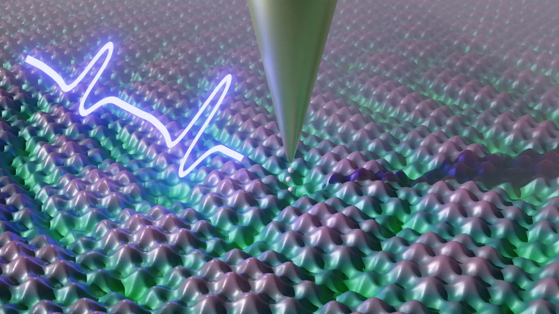
The research led by Prof. Loth’s group focused on a material composed of niobium and selenium, offering a pristine environment to study the collective motion of electrons in a charge density wave. By introducing a single impurity into the mix, the scientists observed how this disruption halted the collective electron movement. Employing an ultra-short electrical pulse lasting a mere picosecond, the researchers induced nanometer-scale distortions that triggered intricate electron dynamics within the material, shedding light on the interplay between impurities and material properties.
The implications of this research extend beyond fundamental science to practical applications in materials design. By unraveling the mechanisms that govern electron behavior at the atomic level, scientists can engineer materials with tailored properties efficiently. Imperfections such as impurities play a crucial role in dictating material performance, and understanding their impact allows for precise manipulation to achieve desired technical outcomes. Prof. Loth emphasizes the pivotal role of atomic-level design in shaping macroscopic material properties, paving the way for innovative technologies like ultra-fast switching materials for sensors and electronic components.
Traditionally, visualization techniques were limited to achieving either high spatial resolution or high temporal resolution, but not both simultaneously. The novel approach adopted by Prof. Loth and his team combines a scanning tunneling microscope, renowned for its atomic-level resolution, with pump-probe spectroscopy, a method known for its ultrafast temporal capabilities. This synergy enables the researchers to capture detailed electron movements with unprecedented precision, offering a holistic view of material dynamics at the atomic scale.
However, achieving such precise measurements comes with its challenges. The laboratory setup must be meticulously shielded against vibrations, noise, and fluctuations in temperature and humidity to capture the weak signals emitted during the experiments. Prof. Loth underscores the importance of repeated measurements to ensure accurate results, disclosing that their optimized microscope can conduct the experiment a staggering 41 million times per second, setting a new benchmark in signal quality.
The development of quantum microscopy by Prof. Sebastian Loth and his team at the University of Stuttgart represents a significant leap forward in our understanding of material behavior at the atomic level. By unraveling the intricate dance of electrons within advanced materials, this research not only expands the frontiers of scientific knowledge but also opens up pathways for the design of novel materials with tailored properties. The fusion of high spatial and temporal resolution in the Stuttgart microscope heralds a new era in materials science, with potential applications ranging from advanced sensors to ultrafast electronic components.
Leave a Reply