
The field of electronics is constantly evolving, with researchers looking for innovative materials to push the boundaries of performance even further. One such material gaining attention is two-dimensional (2D) semiconductors, which have properties that make them promising candidates for enhancing the capabilities of electronic devices. Despite their potential, 2D semiconductors face challenges, such as high contact resistances, that limit their use in transistors.
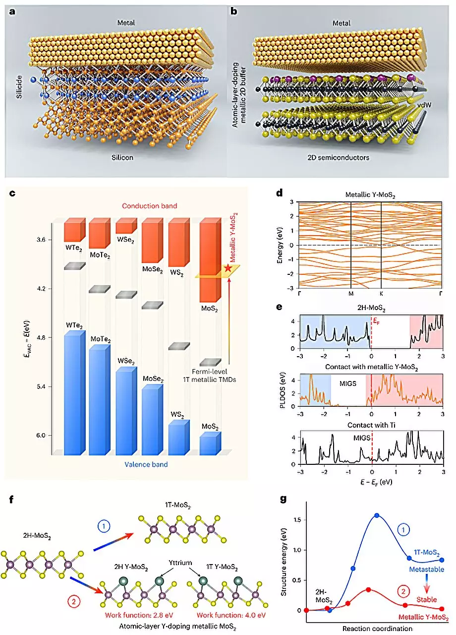
Recently, researchers at Peking University and Chinese Academy of Sciences have introduced a new yttrium-doping strategy aimed at overcoming the limitations of 2D semiconductors. By doping semiconducting molybdenum disulfide (MoS2) with yttrium, the researchers were able to enhance band alignment and improve the performance of MoS2 in fabricating ohmic contacts for 2D transistors.
One key aspect of the yttrium-doping strategy is the use of the plasma-deposition-annealing method to achieve doping in the MoS2 material. This process involves treating patterned local contact areas with low-power soft plasma to generate active sites, followed by the deposition of a Y/Ti/Au stacked metal. The 1 nm-thick active metal Y serves as a solid-state doping source, with Y atoms diffusing into the active sites and being activated through high-temperature annealing.
The introduction of yttrium doping led to a phase transition in the MoS2 material, resulting in improved performance in ultra-short MoS2-based channel ballistic transistors. These transistors displayed excellent switching capabilities and performed well as ohmic contacts, showcasing the potential of the yttrium-doping strategy in advancing 2D semiconductor technology.
Looking ahead, the researchers aim to develop equally excellent p-type ohmic contacts suitable for 2D semiconductors, further expanding the applications of the yttrium-doping strategy. The development of new sub-1 nanometer node chips with remarkable performance and lower power consumption could be on the horizon, thanks to the advancements in 2D semiconductor technology.
The yttrium-doping strategy introduced by researchers represents a significant step towards addressing the limitations of 2D semiconductors and enhancing their performance in electronic devices. By leveraging innovative techniques such as plasma-deposition-annealing and achieving a phase transition in the material, the researchers have paved the way for the development of next-generation transistors with improved capabilities. As the field of electronics continues to evolve, it is efforts like these that drive progress and pave the way for future advancements in technology.
Volcanoes, while majestic, pose significant risks to human life and infrastructure due to their unpredictable…
In the quest for sustainable energy solutions, the focus has sharply turned to the promise…
Cancer, often perceived solely as a physical affliction, embeds deeper psychological shadows within its victims,…
Scientific progress often hinges on revolutionary ideas that challenge the status quo, and it is…
In the vast cosmos, black holes have long tantalized astronomers and astrophysicists alike with their…
In a groundbreaking leap that could redefine computing as we know it, researchers at Skoltech,…
This website uses cookies.
