
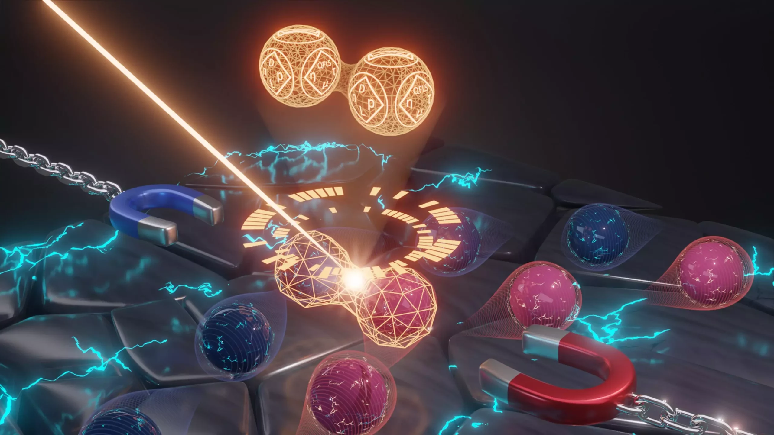
An innovative new method for the comprehensive characterization of semiconductors has been developed by a physicist at HZB. The “Constant Light-Induced Magneto-Transport (CLIMAT)” method is a groundbreaking technique that allows for the simultaneous recording of 14 different parameters of transport properties of both negative and positive charge carriers in a single measurement.
Traditionally, the parameters of transport properties in semiconductors had to be determined separately for each type of charge using different measurement methods. However, the CLIMAT method streamlines the process by utilizing the Hall effect, a magnetic field, and a constant light source for charge separation. This innovative approach provides a comprehensive insight into the complex mechanisms of charge transport, enabling researchers to evaluate new semiconductor materials much more quickly for various optoelectronic applications.
The versatility of the CLIMAT method has been demonstrated through the characterization of twelve different semiconductor materials, including silicon, halide perovskite films, organic semiconductors, semi-insulators, self-assembled monolayers, and nanoparticles. The results of these studies have been published in Nature Communications, showcasing the broad applicability of the new method across various types of semiconductor materials.
Independent experts, such as Prof Vitaly Podzorov from Rutgers University, have awarded the CLIMAT method high praise and consider it to be groundbreaking in the field of semiconductor characterization. The method has also been approved for patenting by the European Patent Office, signaling its potential for commercialization. Negotiations are currently underway with companies for licensing the method, with the ultimate goal of developing a compact measuring device the size of a notebook.
The development of the CLIMAT method represents a significant advancement in the field of optoelectronics, offering researchers a more efficient and comprehensive way to characterize semiconductor materials. With its ability to provide detailed insights into the behavior of both positive and negative charge carriers, the CLIMAT method holds great promise for accelerating the development of new materials for applications such as solar cells, transistors, detectors, sensors, and LEDs. The potential impact of this innovative technique on the field of semiconductor research is vast, paving the way for new discoveries and advancements in optoelectronics.
Rogue waves have long been a subject of fascination and terror in maritime lore. These…
As the world grapples with public health challenges, especially those posed by infectious diseases, the…
The Sombrero Galaxy, also known as Messier 104, embodies a breathtaking blend of spirals and…
In recent advances in quantum electronics, a groundbreaking discovery leveraging the concept of kink states…
In the intricate tapestry of nature, ice often exists in a delicate balance with liquid…
In an astonishing event that captured global attention, a rogue object from beyond our Solar…
This website uses cookies.